Physics and Electro-Optics
Optical Bus for a Multi-Core Processor (No. T4-1863)

5704
Overview

Over the last decades, the exponential increase in computational power is running into a bottleneck, as integrating multiple cores is currently the most efficient way to get more computing power per chip. However, multiple-core architecture demands a complex wiring system for inter-core communication. The technology presented here proposes a radically new idea that replaces wires with an appropriately designed integrated optical chip layer using the power of silicon photonics (SiPh). Wiring elimination saves valuable space and reduces power consumption and internal heat production. This technology allows a high number of interconnected processors on the same chip and improves inter-core connectivity up to 1000-fold, thus increasing computational power.

The Need

Chipmakers are constantly seeking innovative ways to reduce power consumption, heat production, and component volumes of compact electronics. Technology developments have increased the end-user demands for faster and more efficient systems, requiring either improved clock-speed or multicore processors and subsequent complex inter-core communication. Both alternatives suffer significant drawbacks, as increased clock speed results in higher power consumption and internal heat production, while efficient inter-core communication using complex wire bus systems takes up space, consumes energy, and produces excess heat. Optical fibers are currently the best solution in the market for internal heat reduction. However, they are still limited by complex wiring networks and one-dimensional optical data transmission. There is a need for a more efficient, less complex solution that will enable better multicore processor connectivity.

The Solution

A single compact on-chip optical layer, compatible with CMOS fabrication technologies, that replaces the tangle of wires and fibers in multicore processors. 

Technology Essence

This invention involves a compact optical bus that is comprised of a planar waveguide on silicon chips, where light is confined in a layer by total internal reflection. The layer is made of silicon sandwiched between silica layers (glass), while the inner silicon layer has a high refractive index compared to the upper and lower silica layers. The height of the highly refractive layer is carefully designed to provide a specific refractive index profile dictated by the layer thickness. A light management system selectively activates specific illumination ports embedded within the waveguide; the emanating light is then focused onto reflectors (Bragg mirrors), leading to light ray emission at specific partner points. The light can be simultaneously focused onto a plurality of photodetectors within the waveguide, each communicating with a separate processor core. The optical bus can be designed in several geometries, reaching very high core densities, and can be adjusted to match computer processor or core layout requirements to overcome the need for physical wiring (see Figure below). 

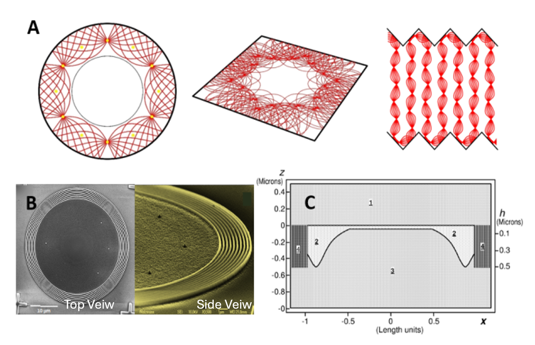
A) Schematic top view of a propagation layer of the optical bus depicting light propagation from a divergence point to convergence at multiple focal points for a circular (left), square (middle), or spiral (right) embodiment of the optical bus. B) A top view (left) and a side view (right) of a prototype manufactured by an e-beam lithography taken with electron microscope. C) Schematic cross-sectional view of an optical bus. Upper (1) and lower (3) non-propagation layers; light propagation layer (2), and a Bragg mirror (4). The effective refractive index defined by the thickness profile of the propagating silicon layer causes light propagation to follow specific propagation paths with unique and exclusive sets of focal points.

Applications and Advantages

Advantages

  • Direct and wireless inter-core communication in multiprocessors using advanced SiPh technology
  • Waveguide fabrication is compatible with traditional CMOS fabrication technologies
  • Scaled-up connectivity of processor cores by up to 1000-fold 
  • Increased computing power 
  • Reduced electric power consumption and heat output
  • Point-to-point communication without crosstalk


Applications

The proposed innovation is applicable for a full range of markets integrating electronic technologies, including: 

  • Consumer electronics 
  • Automotive
  • Hardware for deep-learning networks 
  • Robotics
  • Signal processing
  • Telecommunication
  • Information processing
Development Status

Miniature prototypes have been fabricated (Published in: O. Bitton, R. Bruch, and U. Leonhardt, Phys. Rev. Applied 10, 044059 (2018)), and additional simulations successfully demonstrated high density geometries.  
The prototypes demonstrated the manifestation of the optical bus for inner communication without interconnected wires or fibers, however, to achieve its full potential, it requires prototypes connected externally to many lasers and detectors.


Patent Status: 
USA Granted: 10,938,486
Full Professor Ulf Leonhardt

Ulf Leonhardt

Faculty of Physics
Physics of Complex Systems
All projects (1)
Contact for more information

Nir Stein

Director of Business Development, Exact Sciences

+972-8-9345164 Linkedin