Inertial sensors for motion detection are increasingly integrated into portable devices, including IoT applications, mobile phones, wearables, automotive systems, and medical diagnostics. The demand for smaller electronics is driving innovation in miniaturized components. This technology introduces a novel nanoscale inertial sensor based on the piezoresistive effect. It features a suspended nanotube with an offset pedal that generates an electrical signal in response to motion, enabling accurate and efficient motion sensing across a range of applications.
- IoT devices and smart sensors
- Navigation systems and motion tracking
- Wearable electronics (e.g., smartwatches, fitness trackers)
- High-resolution camera stabilization
- 3D gaming and augmented reality
- • Medical implants and diagnostic devices
- Nanoscale design – Ultra-miniaturized sensor with pedal dimensions >250×500 nm
- Electrical signal output – Enables seamless integration with electronic systems
- Durability and reliability
- High sensitivity – Torsional resonance frequency of 20 ± 4 MHz for precise motion detection
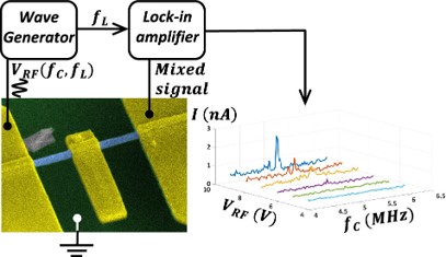
Scanning electron microscope of the inorganic nanotube-based self-sensing torsional resonator (left). The inertial sensor is actuated by applying voltage between the substrate and the offset pedal, which is attached to the nanotube. Piezoresistive enables direct electrical detection of the resonance spectrum (right)
A self-sensing torsional NEMS resonator has been successfully demonstrated. Proof-of-concept prototypes of NEMS accelerometers and gyroscopes are under development.


Dr. Vered Pardo Yissar